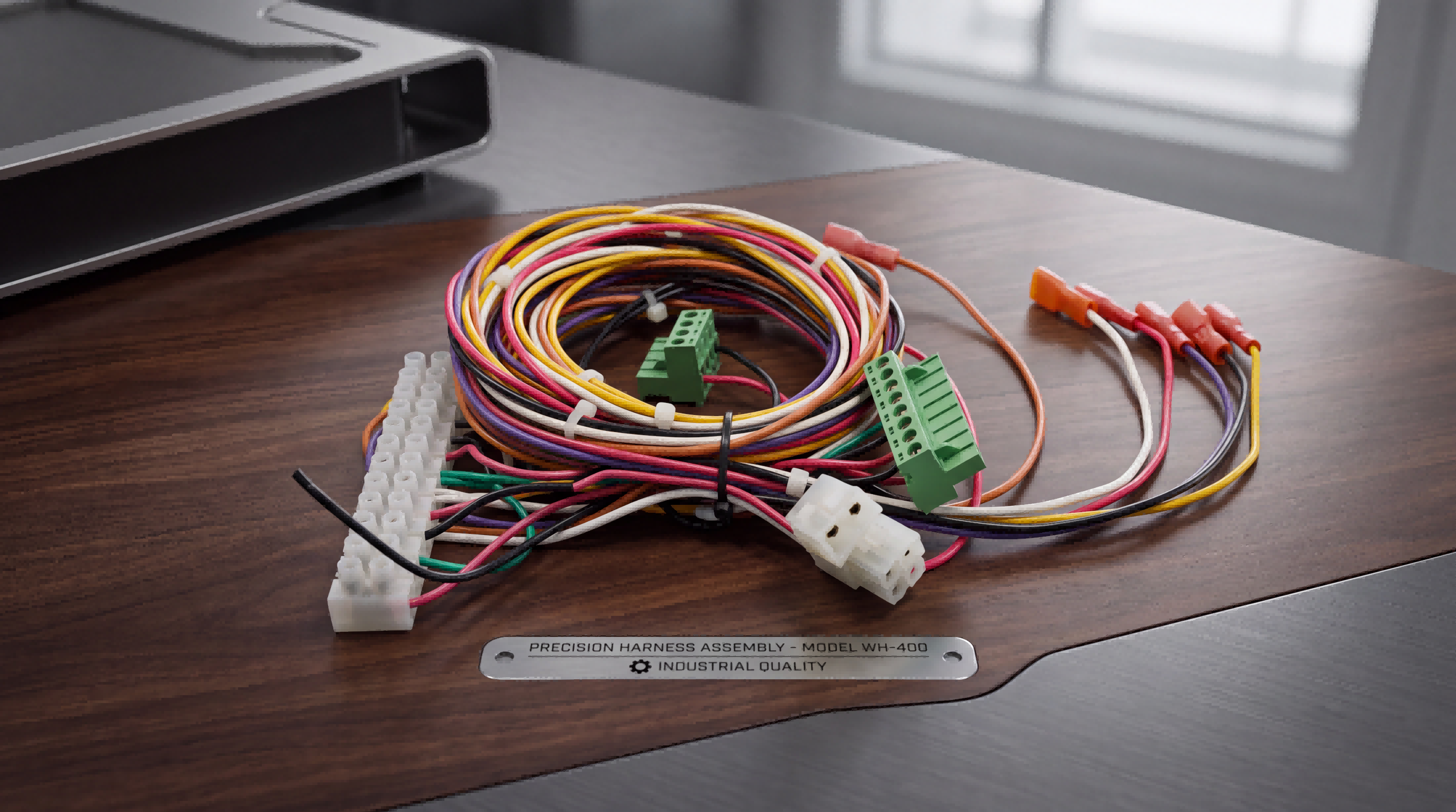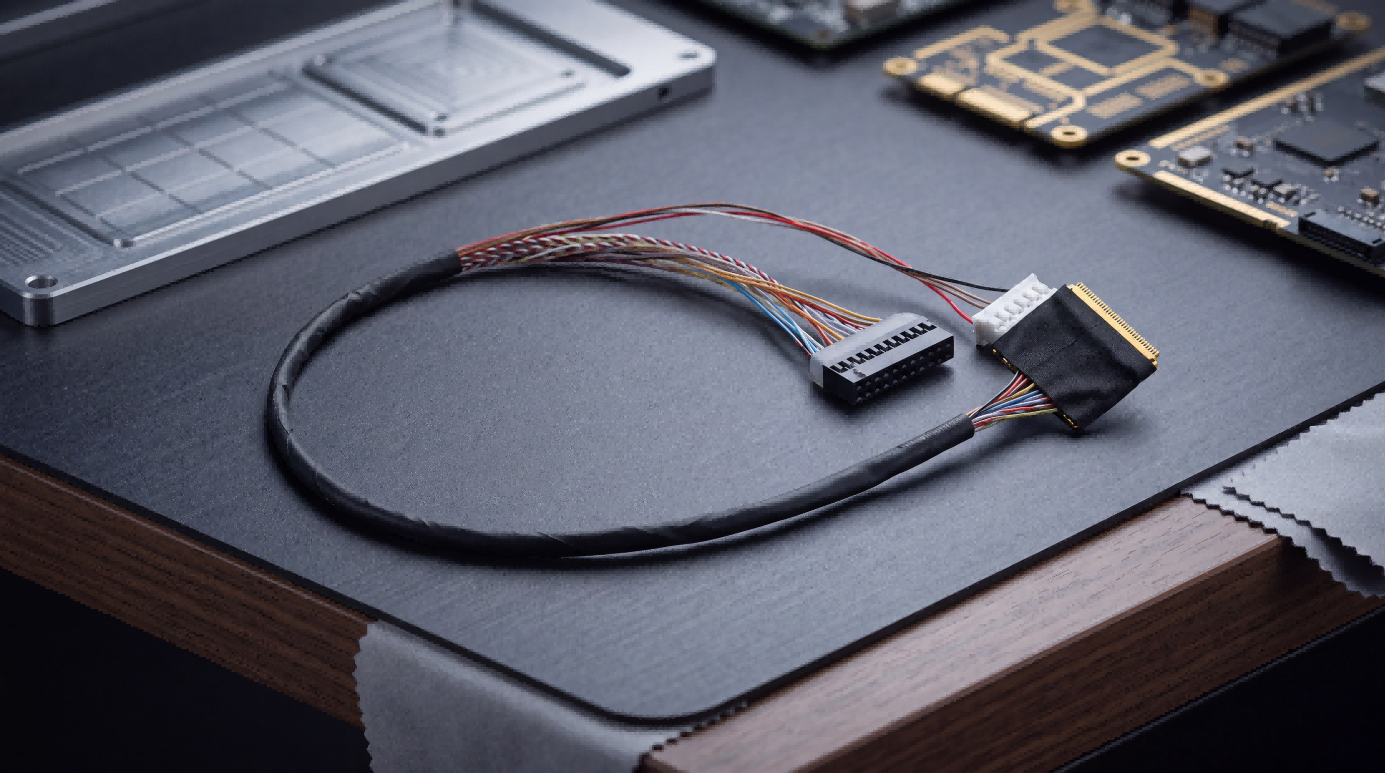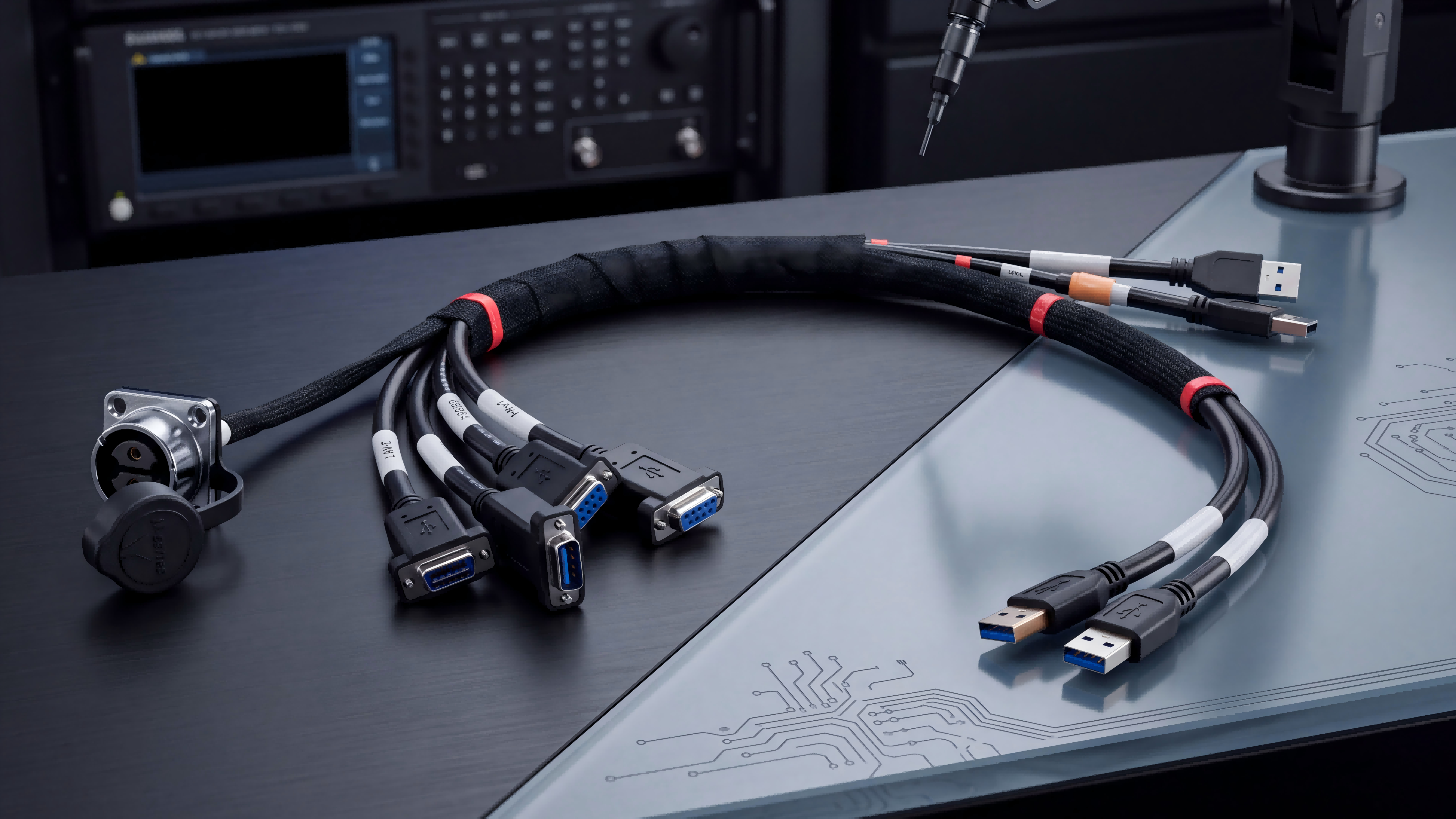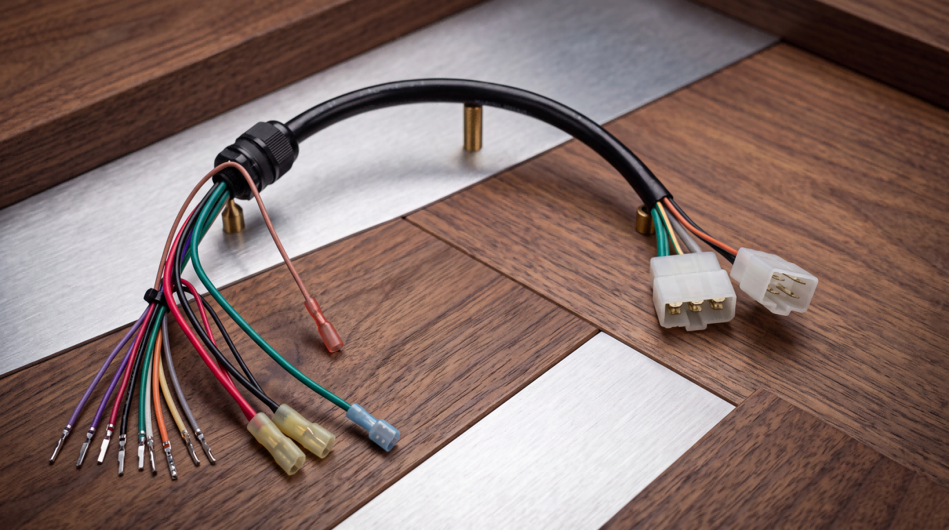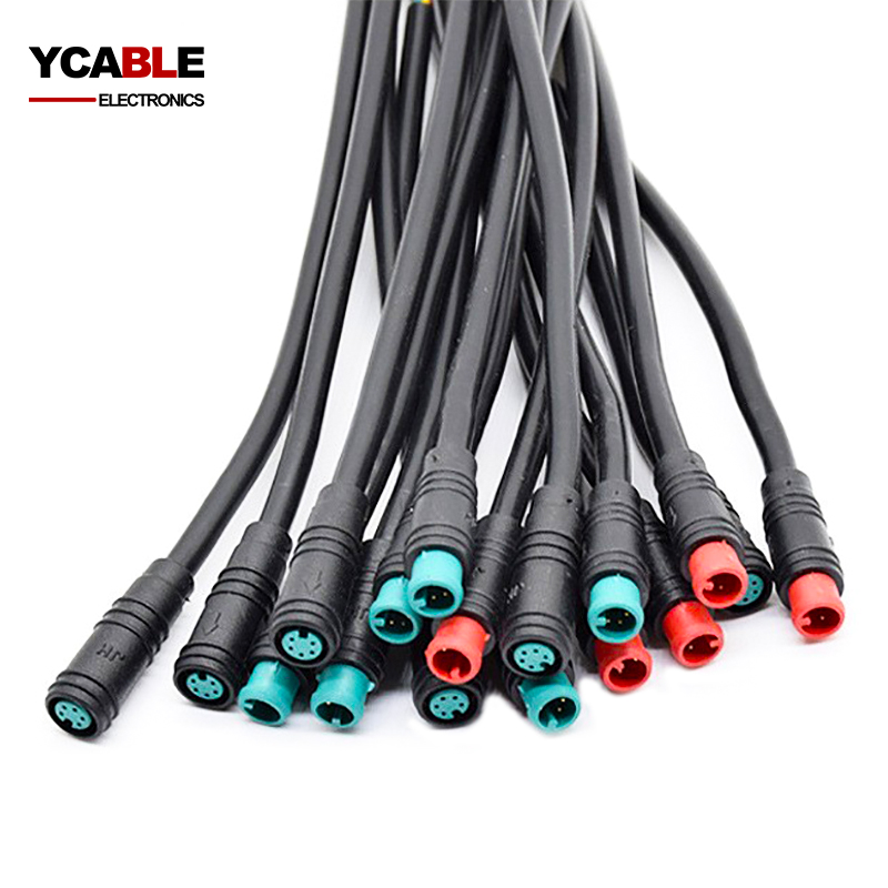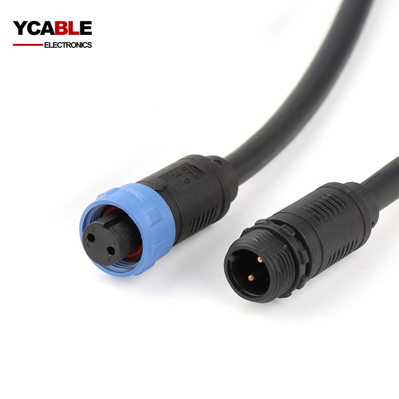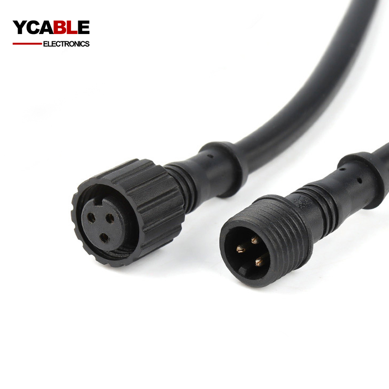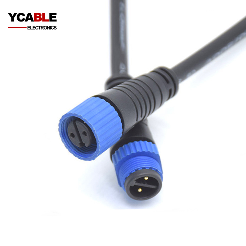
Custom Semiconductor Equipment Wiring Harness Solutions
The Ultimate Guide to Semiconductor Equipment Wiring Harness Solutions: Securing Wafer Yield and Uptime
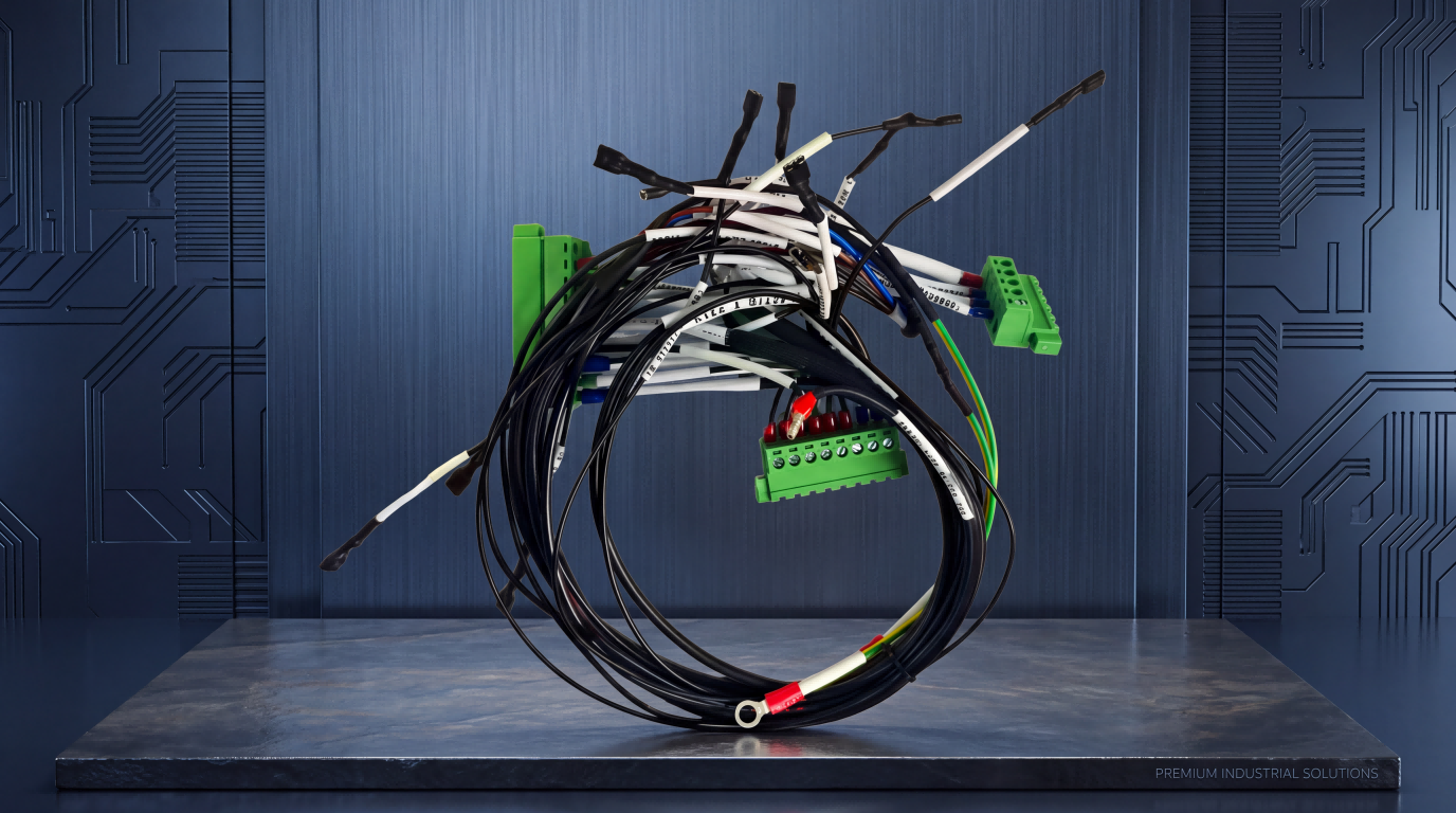
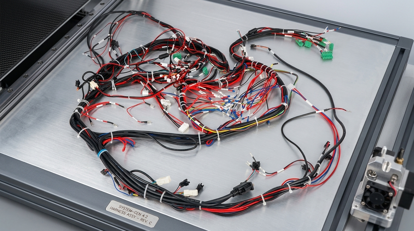
In the highly competitive field of semiconductor manufacturing, precision and reliability are not merely expectations—they are strict prerequisites. Equipment uptime and wafer yield are the ultimate metrics that define a fabrication plant's profitability. At the heart of this complex machinery lies a critical, yet often overlooked component: the semiconductor equipment wiring harness. Acting as the central nervous system of semiconductor fabrication plants (fabs), these advanced cable assemblies ensure flawless power transmission and high-speed signal interaction under the most demanding conditions.
From extreme vacuum environments to exposure to strong corrosive chemicals, a standard cable simply cannot survive. This article delves deep into the core concepts, technical specifications, and industrial applications of the semiconductor device wiring harness, providing purchasing managers and R&D engineers with the insights needed to make informed sourcing decisions.
Core Concepts: Defying Extreme Environments
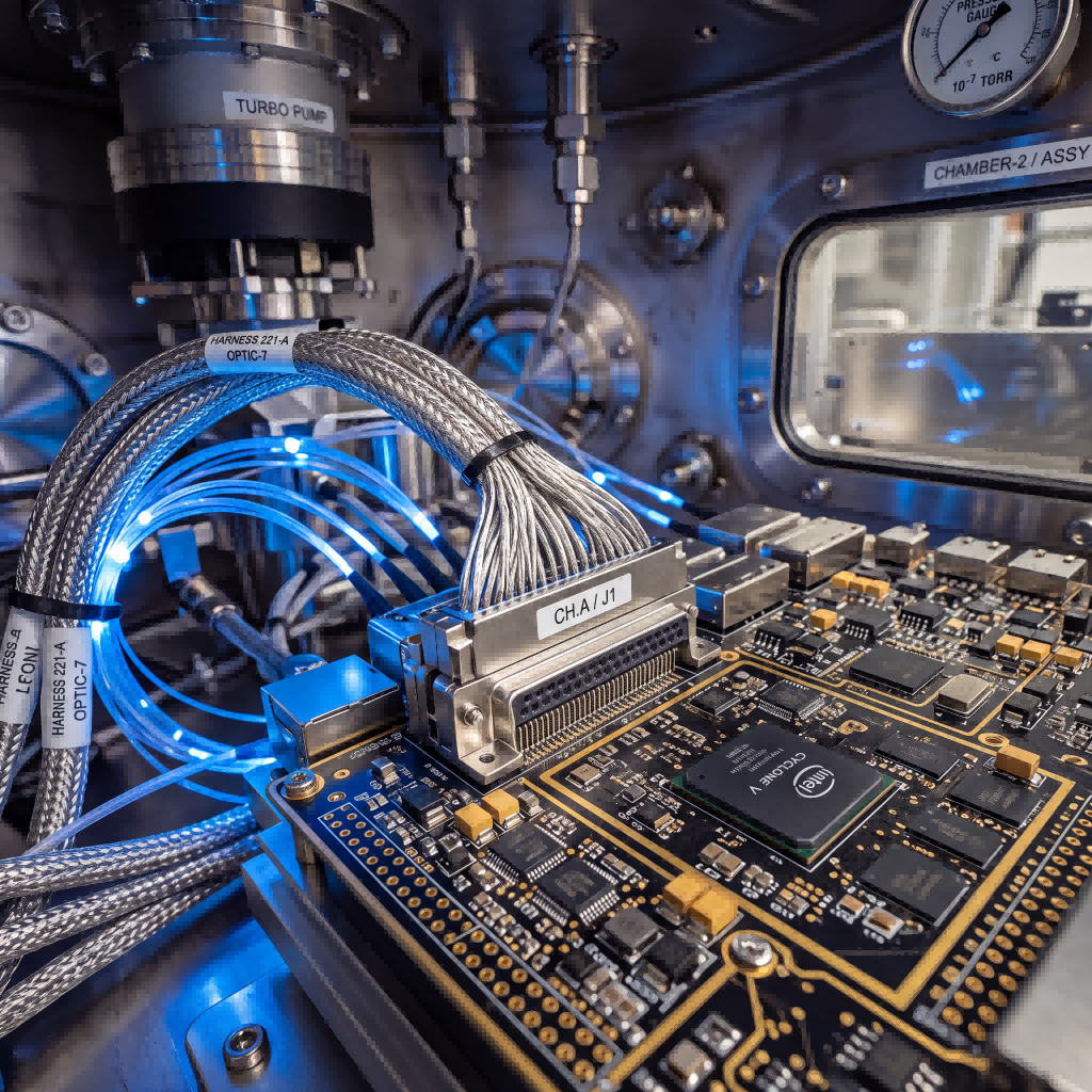
A semiconductor equipment connection harness is engineered specifically to operate flawlessly within the harsh confines of wafer processing equipment. Unlike standard industrial cables, these harnesses must prevent outgassing in ultra-high vacuum (UHV) environments, which could otherwise contaminate silicon wafers and drastically reduce yield rates.
Furthermore, processes like Chemical Vapor Deposition (CVD) and plasma etching expose the semiconductor equipment internal wiring harness to aggressive chemicals and extreme temperatures. High-grade materials such as PTFE (Teflon) and specialized FEP insulation are required to provide robust chemical resistance. By maintaining high-frequency data transmission integrity and stable power delivery without degradation, these harnesses directly safeguard equipment Overall Equipment Effectiveness (OEE) and maximize continuous production capabilities.
Technical Classification, Features, and Applications
The architecture of a semiconductor manufacturing equipment wiring assembly is highly customized based on the specific module it serves within the fab. Understanding the different classifications helps procurement specialists source the exact match for their engineering needs.
1. High-Power Transmission Harnesses
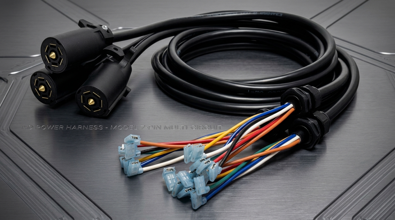
- Features: Built with high-purity oxygen-free copper (OFC) and multi-layered shielding to handle high voltage without overheating or electromagnetic interference (EMI).
- Working Principle: Delivers stable, unfluctuating power to heavy-duty modules like ion implanters and heating stages.
- Application Scenario: Essential for powering the magnetrons and RF generators inside physical vapor deposition (PVD) tools.
2. High-Frequency Signal and Control Harnesses
- Features: Incorporates twisted pairs with individual aluminum foil shields and tinned copper braiding. Low dielectric constant materials are used to minimize signal attenuation.
- Working Principle: Ensures nanosecond-level precise communication between the central PLC and robotic wafer-handling arms.
- Application Scenario: Widely utilized in photolithography machines where micron-level alignment relies on instant, noise-free sensor feedback.
3. Vacuum and Chemical Resistant Sensor Harnesses
- Features: Wrapped in extruded fluoropolymer jackets with zero outgassing properties. Non-reactive to plasma and etching gases.
- Working Principle: Connects internal chamber sensors (temperature, pressure, gas flow) to exterior monitors without breaking the vacuum seal via hermetic feedthroughs.
- Application Scenario: Deployed directly inside dry etching chambers and atomic layer deposition (ALD) systems.
Essential Specifications for Semiconductor Cable Assemblies
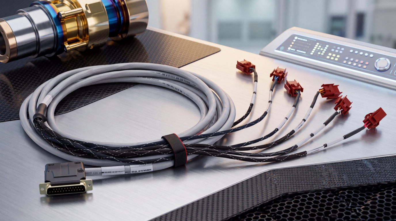
To guarantee absolute performance, a top-tier semiconductor equipment cable harness must adhere to rigorous electrical and mechanical specifications. Below are the standard technical parameters required for fab-grade applications.
Wire Specifications
| Parameter | Specification Details | Industry Benefit |
|---|---|---|
| Conductor Material | High-Purity Silver-Plated Copper / Tinned Copper | Ensures high-speed signal integrity & corrosion resistance |
| Insulation Material | PTFE, FEP, PFA (Fluoropolymers) | Zero outgassing, withstands temperatures up to 260°C |
| Shielding Type | Double Shielding (Al-Mylar Foil + Copper Braid) | >95% EMI/RFI rejection for error-free data logic |
| Voltage Rating | 300V / 600V / 1000V (Customizable) | Safe power delivery across varying equipment modules |
| Temperature Range | -200°C to +260°C | Operational stability in cryogenic and heating stages |
Connector Specifications
| Parameter | Specification Details | Industry Benefit |
|---|---|---|
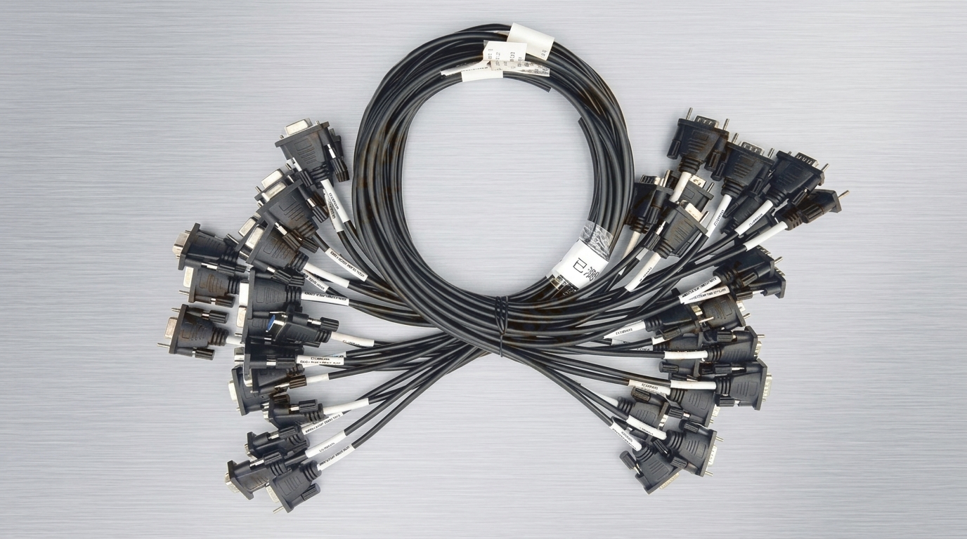
| Connector Type | MIL-Spec, D-Sub, Circular, Hermetic Feedthroughs | Standardized compatibility with global fab equipment |
| Contact Material | Beryllium Copper with Heavy Gold Plating (30µ" to 50µ") | Low contact resistance, withstands thousands of mating cycles |
| Housing Material | Stainless Steel 316L, High-Temp PEEK | Resistant to strong acids, bases, and plasma degradation |
| Sealing Standard | IP67 / IP68 / Ultra-High Vacuum (UHV) rated | Prevents microscopic particle contamination and leaks |
| Durability | Minimum 5,000 Mating Cycles | Reduces maintenance downtime and replacement costs |
Your Trusted Partner for Wiring Harness Solutions
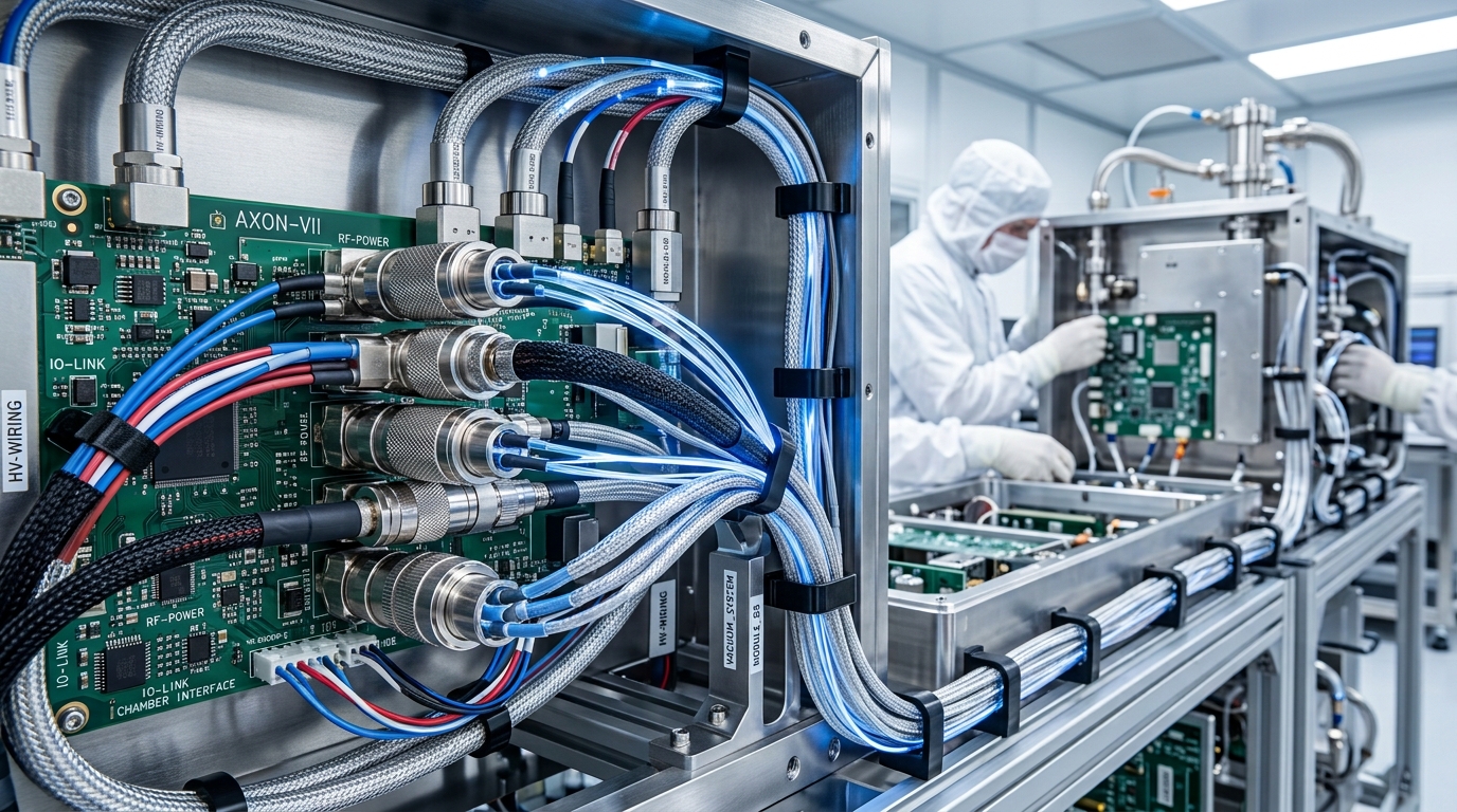
As a premier custom wiring harness manufacturer, we understand the zero-tolerance policy for failure in the semiconductor industry. Our manufacturing facility is strictly ISO9001 certified, ensuring every semiconductor equipment wiring harness that leaves our cleanrooms meets the highest global standards for quality and trace-ability.
We offer comprehensive custom/OEM/ODM support tailored to the precise schematics of your equipment. Whether you are developing next-generation EUV lithography machines or upgrading existing CMP tools, our professional design team provides complete solutions from initial blueprint drafting, prototype validation, to final mass production.
Understanding the dynamic nature of semiconductor R&D, we proudly support small batch production for engineering verification testing (EVT) and pilot runs, allowing rapid iteration without the burden of massive Minimum Order Quantities (MOQs).
Ready to Upgrade Your Equipment's Reliability?
Do not let substandard cabling be the bottleneck of your equipment's performance. Partner with us for robust, contamination-free, and precision-engineered connectivity. Contact our engineering team today to discuss your specifications, request a custom quote, and discover how our advanced wiring solutions can elevate your semiconductor manufacturing equipment to the next level of operational excellence.